The goal of this PCB was to create a compact PCB that can control all the aspects of Autonomous flight. This includes sensors such as IMU, Barometer, and GPS, communication via LoRa and ELRS, and power control for both a motor battery and a designated PCB battery.
Key Engineering Challenges:
I²C reliability
Power management complexity
RF signal integrity
High-current servo power routing
Iteration from V1.0 to V1.1
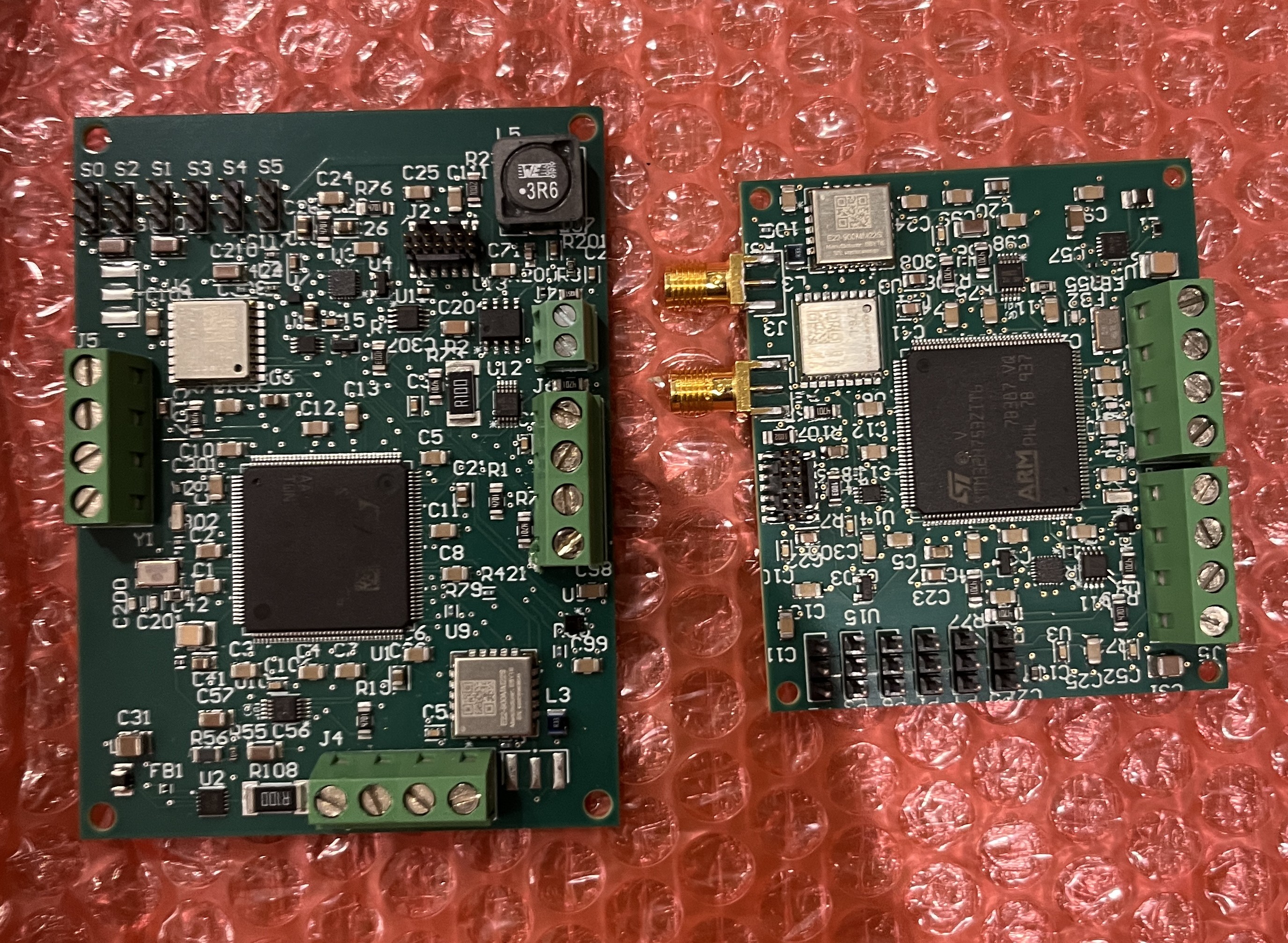
V1.0 PCB vs V1.1 PCB
Version 1.0:
Figure 1: V1 PCB.
Schematic Design:
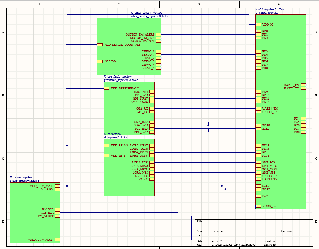
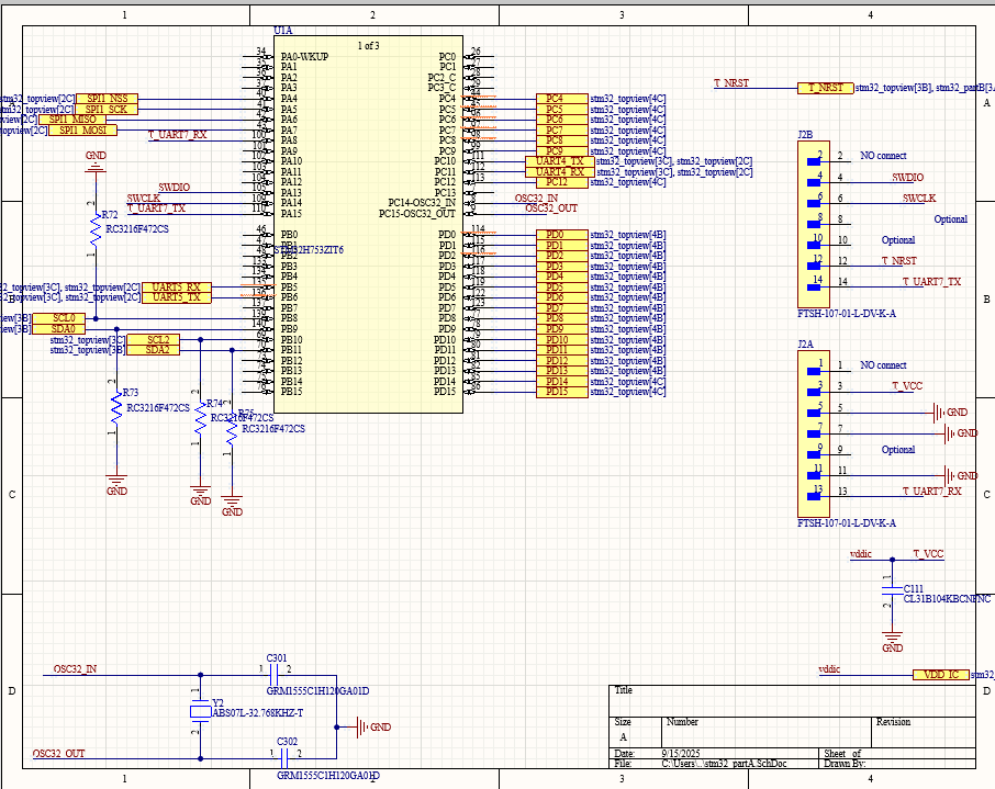
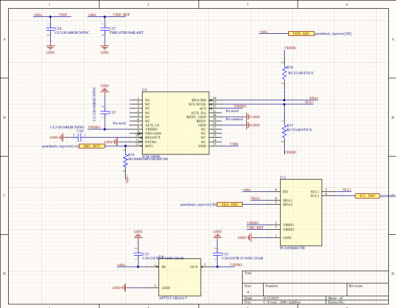
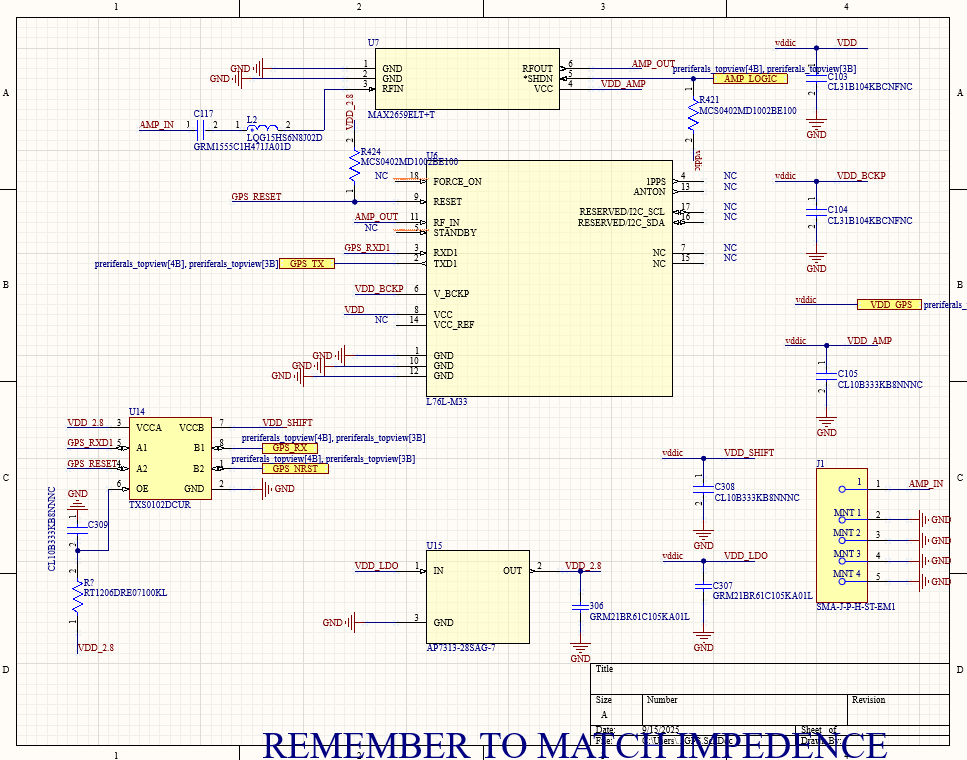
I designed this PCB in Altium Designer, using surface-mount parts for a compact design and maximum customization. First, I picked the STM32H7 series processor because it offers 2MB of flash and 1MB of RAM in a small package. Then, I made an overview of what I needed and came up with GPS, LoRa, ELRS (for manual override), IMU, Barometer, Servos, and Power monitoring. After selecting all these components, I used the datasheets to wire them correctly and a Hierarchical design in Altium to keep everything organized. I chose to use one battery dedicated to my PCB, sensors, and radios, and another for the motor and servos. Both of these were connected to the PCB; the motor battery provided 5V to the servos and my ELRS module via a buck-and-boost converter. This strategy to regulate 5V on board proved unwise, adding complexity and board heat, necessitating a V1.1. I used a Silicon-Ion battery because its energy density is almost double that of a normal LiPo. All the batteries have power filters using ferrite beads and bulk decoupling capacitors. They also have monitors that use an INA226 to read and transmit the battery status. I mainly chose components that communicated via I2C to use fewer pins and make routing easier. Finally, I used ST-Link for code flashing and debugging, as it works very simply with an STM32.
Figure 2: Complete schematic overview of V1.0.Figure 3: STM32 microcontroller section of the schematic.Figure 4: IMU sensor schematic section.Figure 5: GPS module schematic section.
PCB Layout:
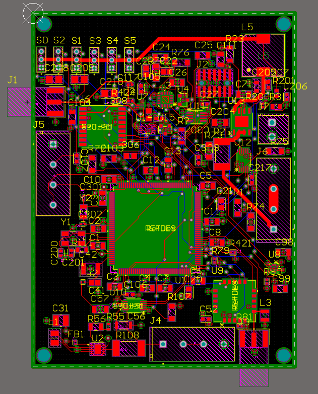
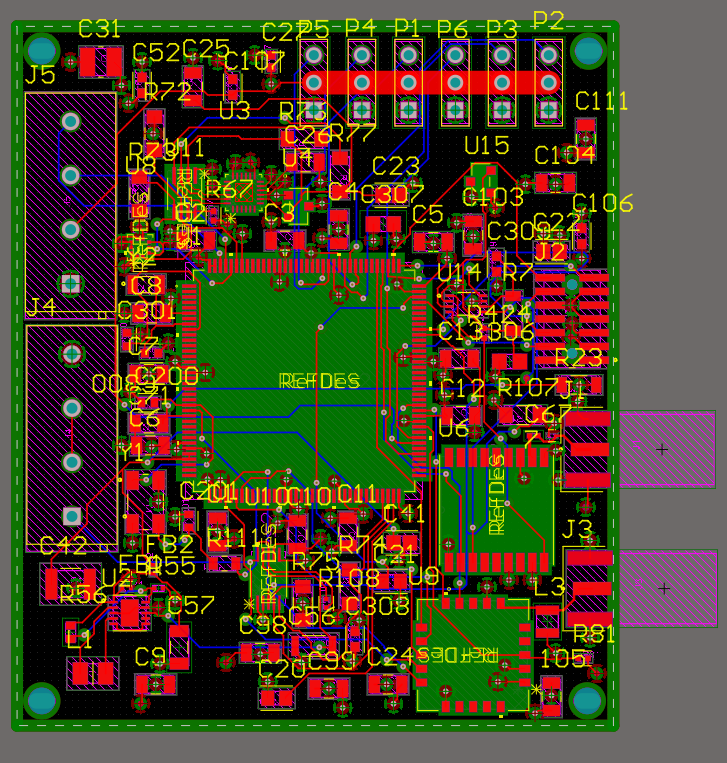
For the PCB layout, I chose a 4-layer board to dedicate two signal layers, a 3.3V plane, and a GND plane. Firstly, I put my STM32 in the center, and all the radio modules on the sides of the board. This was because my SMA connectors needed to stick out the sides of the board, so the corresponding modules needed to be close. I made sure to keep traces short, especially for essential signals like I2C and RF. I calculated the trace widths to ensure everything has 50 ohm impedance and created specific RF areas with no other signals routed. This reduced the noise from surrounding traces and components on my RF modules. Next, I routed my main 5V power into large traces, since servos can draw a lot of power, which can cause small traces to heat. Finally, I made sure there were no right angles or extreme curves to ensure signals are reliable. Throughout this time, I used Altium's auto-BOM and a spreadsheet to track what I needed to buy.
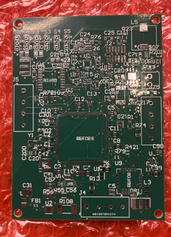
Figure 6: The PCB routing and layout view.Figure 7: Bare PCB V1.0.
Fabrication & Assembly:
This board was manufactured and assembled by PCBWay. I chose to switch from JLCPCB to PCBWay because JLCPCB's assembly service would not order parts they did not have in stock. I decided to have my board professionally assembled because the components I chose were tiny. I also did not have the proper Hot Air Rework station and fine motor control to do it myself.
Firmware:
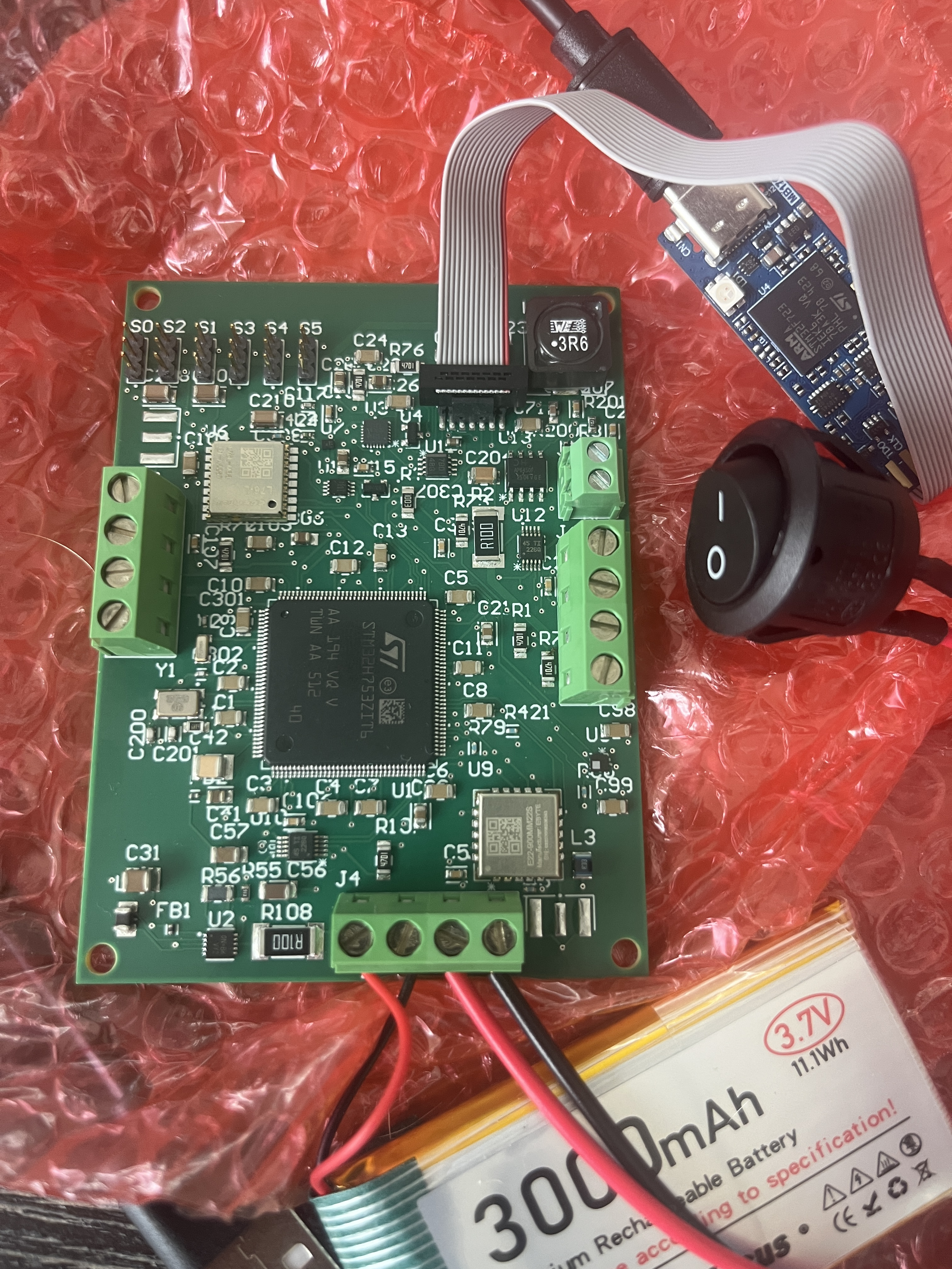
This section focuses only on hardware bring-up and component testing. Early on, I discovered that my I2C lines were pulled down rather than pulled up, preventing me from testing the devices that relied on I2C. Despite that, I was able to test the LoRa module, GPS module, and servos. Both radio modules communicated correctly and searched for valid signals. However, I could not attach the antennas because the SMA connectors were placed too far from the board's edge to solder correctly. The servos also worked as expected using PWM. During testing, I also found that my 5V regulation failed due to a broken resistor. Finally, I gained a lot of information when my STM32 worked as expected, and I was able to flash code successfully after configuring the clock.
Figure 8: The firmware project file structure.Figure 9: Uploading code to the flight controller.
Challenges:
In version one, I ran into several challenges that led to partial failures. This was my first time using Altium Designer and building a surface-mount-focused board, so I had to learn many things as I went. The first major hurdle was figuring out how to import footprints from online libraries like UltraLibrarian, which took nearly five hours before I finally found the correct import tools. The main technical issue I faced was with my 5V regulation. Even though the regulator failed due to a broken resistor, I also found that regulating 5 V on board caused back-feeding into the STM32, which caused it to heat up. I also ran into problems with my GPS design. I added an onboard LNA, but when choosing an antenna, I found that most available options were active pucks. Using two amplifiers in the same chain would have caused excessive amplification and noise.
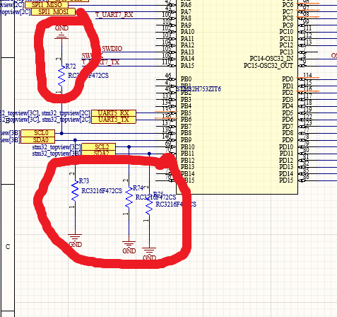
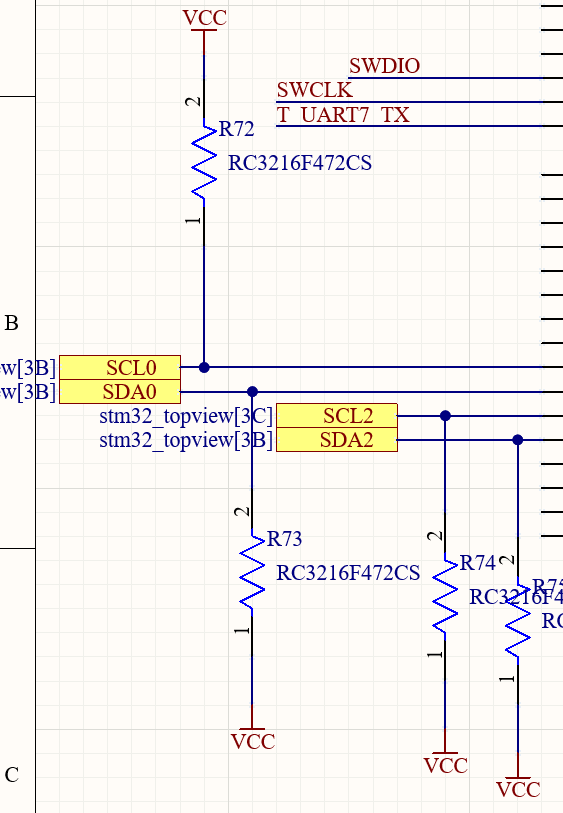
Figure 10: Debugging I2C communication issues during development.
Version 1.1:
Figure 11: 3D render of Version 1.1 PCB.
Version 1.1 Changes:
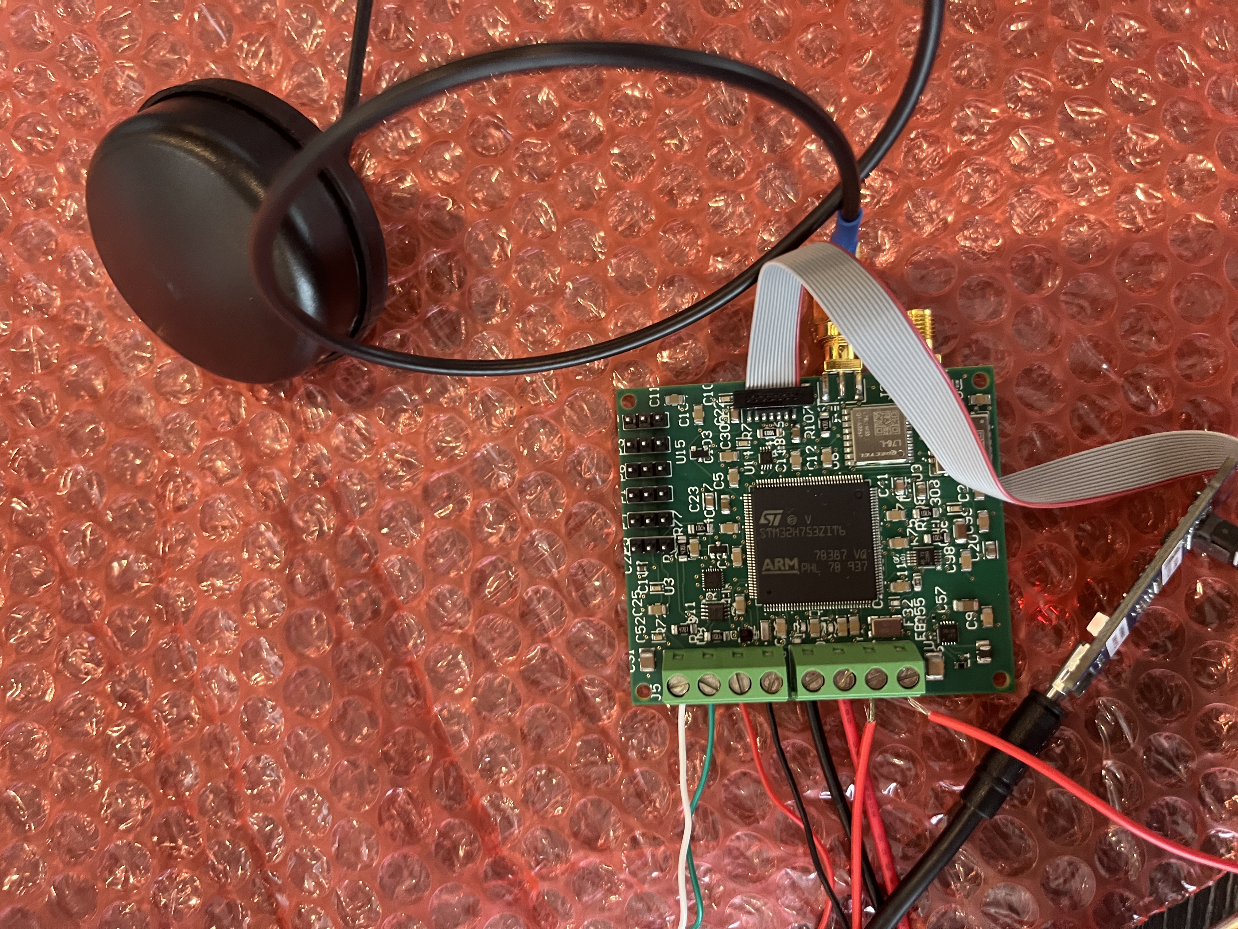
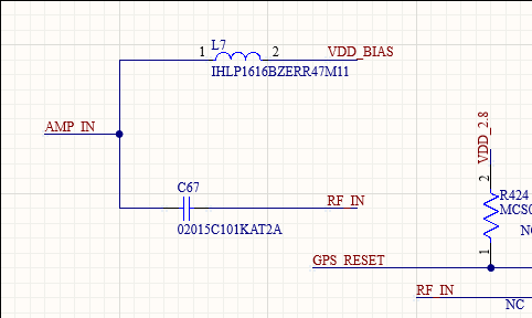
In version two of the PCB, I completely got rid of my onboard 5V regulator due to its added complexity and instead decided to use the 5V BEC on my ESC. This made my design much simpler, as I did not need to worry about high-power regulation or current, instead using an ESC rated for very high current. I still needed large traces for my servo power, since it can draw up to 3A at a time. Next, I removed my on-board LNA and added a bias tee, using an active puck instead, simplifying my design. Furthermore, I changed my 3.3V regulation, as I accidentally used 1000x smaller resistors than needed. It outputs the correct 3.3V, but the buck and boost used 1000x the current than needed. To confirm my design, I used a new strategy: I exported my full wirelist, downloaded the datasheets, and gave all that info to Opus 4.5 and GPT 5.1, which checked it and recommended improvements and fixes, such as different load capacitors for my external clocks on the STM32. For the board design, since I removed many components and simplified everything, I reduced the board size by about 1 inch in both the x and y directions. I also made the servo connectors larger and put the SMA connectors on the edge. Finally, I made sure to pull up my I2C lines. Overall, my V1.1 simplified the design and fixed the errors I encountered while testing V1.
Figure 12: I2C pull-up resistor fix in V1.1.Figure 13: Bias tee for active GPS antenna.Figure 14: Larger servo connectors in V1.1.Figure 15: AI-assisted design verification method.Figure 16: Complete PCB layout for V1.1.
Tools & Technologies:
Altium Designer, STM32H7, I2C and SPI communication, LoRa and ELRS, active GPS with bias-tee, buck and boost regulation, PCBWay assembly, and C/C++ for hardware bring-up.
Outcome:
Version 1.1 has been completed and sent for manufacturing, fixing the major issues from the first revision and simplifying the overall design. Once the board arrives, I will begin full testing. In the meantime, I will continue to work on the CAD.
Reflection:
This part of my Autonomous UAV project has been extremely valuable. I learned to use professional PCB software, create complex designs with surface-mount components, and develop a design for a larger system.